- 您现在的位置:买卖IC网 > Sheet目录2098 > MK2069-04GILFTR (IDT, Integrated Device Technology Inc)IC VCXO CLK TRANSLATOR 56-TSSOP
MK2069-04
VCXO-BASED UNIVERSAL CLOCK TRANSLATOR
VCXO AND SYNTHESIZER
IDT VCXO-BASED UNIVERSAL CLOCK TRANSLATOR
18
MK2069-04
REV J 051310
Note 1: This is the recommended crystal operating range. A crystal as low as 8 MHz can be used, although this may
result in increased output phase noise.
Note 2: The VCXO crystal will be pulled to its minimum frequency when there is no input clock (CLR = 1) due to the
attempt of the PLL to lock to 0 Hz.
Note 3: The minimum practical phase detector frequency is 1 kHz. Through proper loop filter design lower input
frequencies may be possible. Input frequencies as low as 400 Hz have been tested.
Note 4: A higher input clock frequency can be used when RPV divider = 8.
Note 5: The output of RCLK is a positive pulse with a duration equal to VCLK high time, or half the VCLK period.
Note 6: Referenced to ICLK, the skews of VCLK, RCLK and TCLK increase together when leakage is present in the
external VCXO PLL loop filter.
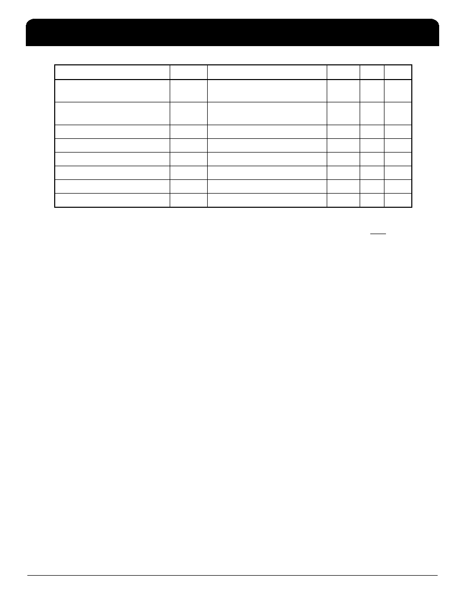
Output Rise Time, VCLK and
RCLK
tOR
0.8 to 2.0 V, CL=15 pF
1.5
2
ns
Output Fall Time, VCLK and
RCLK
tOF
2.0 to 0.8 V, CL=15 pF
1.5
2
ns
Output Rise Time, TCLK
tOR
0.8 to 2.0 V, CL=15 pF
0.75
1
ns
Output Fall Time, TCLK
tOF
2.0 to 0.8 V, CL=15 pF
0.75
1
ns
Skew, ICLK to VCLK (Note 6)
tIV
Rising edges, CL=15 pF
-5
2.5
+10
ns
Skew, ICLK to RCLK (Note 6)
tIV
Rising edges, CL=15 pF
+5
10
+20
ns
Skew, ICLK to TCLK (Note 6)
tVT
Rising edges, CL=15 pF
-5
1.5
+10
ns
Nominal Output Impedance
ZOUT
20
Ω
Parameter
Symbol
Conditions
Min.
Typ.
Max. Units
发布紧急采购,3分钟左右您将得到回复。
相关PDF资料
MK2302S-01LFTR
IC MULTIPLIER/ZD BUFFER 8-SOIC
MK2304S-2LF
IC PLL ZD BUFFER LO SKEW 8-SOIC
MK2703SILF
IC PLL AUD CLK SYNTHESIZER 8SOIC
MK2704SLF
IC PLL AUD CLK SYNTHESIZER 8SOIC
MK2716SLFTR
IC CLK SYNTHESIZER HDTV 8-SOIC
MK2732-06GLF
IC VCXO/MULTIPLIER 16-TSSOP
MK2745-21SLFTR
IC CLK SOURCE DVD/MPEG 16-SOIC
MK2745-24SLF
IC CLK SOURCE DVD/MPEG 16-SOIC
相关代理商/技术参数
MK2069-04GITR
功能描述:IC VCXO CLK TRANSLATOR 56-TSSOP RoHS:否 类别:集成电路 (IC) >> 时钟/计时 - 时钟发生器,PLL,频率合成器 系列:- 标准包装:39 系列:- 类型:* PLL:带旁路 输入:时钟 输出:时钟 电路数:1 比率 - 输入:输出:1:10 差分 - 输入:输出:是/是 频率 - 最大:170MHz 除法器/乘法器:无/无 电源电压:2.375 V ~ 3.465 V 工作温度:0°C ~ 70°C 安装类型:* 封装/外壳:* 供应商设备封装:* 包装:*
MK206N 454634/1/MK
制造商:NSF (CONTROLS) 功能描述:WAFER MK 2POLE 6 POS 制造商:NSF (CONTROLS) 功能描述:WAFER, MK, 2POLE, 6 POS 制造商:NSF (CONTROLS) 功能描述:WAFER, MK, 2POLE, 6 POS; For Use With:Rotary Switches; No. of Poles:2; No. of Positions:6; SVHC:No SVHC (19-Dec-2012); Contact Current @ Contact Voltage AC Max:500mA; Contact Current AC Max:5A; Contact Current DC Max:5A; Contact ;RoHS Compliant: Yes
MK206S 454634MK
制造商:NSF (CONTROLS) 功能描述:WAFER MK 2POLE 6 POS 制造商:NSF (CONTROLS) 功能描述:WAFER, MK, 2POLE, 6 POS 制造商:NSF (CONTROLS) 功能描述:WAFER, MK, 2POLE, 6 POS; No. of Poles:2; No. of Positions:6; SVHC:No SVHC (19-Dec-2012); Contact Current @ Contact Voltage AC Max:500mA; Contact Current AC Max:5A; Contact Current DC Max:5A; Contact Current Rating:5A; Contact ;RoHS Compliant: Yes
MK20-B-100W
功能描述:近程传感器 1 Form A Cylindrical Term.
RoHS:否 制造商:Vishay Semiconductors 感应方式:Optical 感应距离:1 mm to 200 mm 电源电压:2.5 V to 3.6 V 安装风格:SMD/SMT 输出配置:Digital 最大工作温度:+ 85 C 最小工作温度:- 25 C 系列:VCNL3020
MK20-B-100W_DE
制造商:MEDER 制造商全称:Meder Electronic 功能描述:(deutsch) MK Reed Sensor
MK20-B-500W
制造商:MEDER 制造商全称:Meder Electronic 功能描述:MK Reed Sensor
MK20-B-500W_DE
制造商:MEDER 制造商全称:Meder Electronic 功能描述:(deutsch) MK Reed Sensor
MK20-C-100W
制造商:Willow Technologies 功能描述:MICRO REED SENSOR